PCB Assembly Prototype
PCB Assembly Services
Low-Volume PCB Assembly
Turkey PCB Assembly
SMT Stencil
Product Package
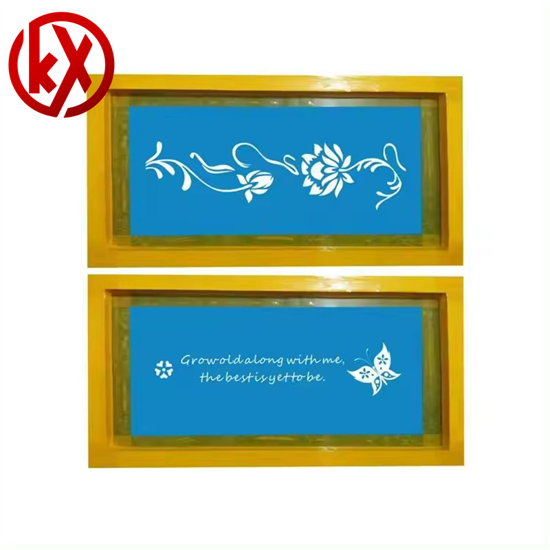
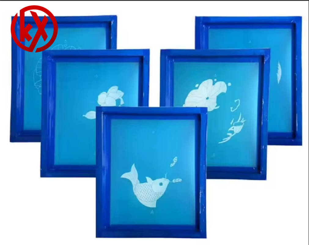
PCB Silkscreen and Soldermask Stencil
Main Equipments
FAQs
PCB Capacity
Multilayer PCB
Flexible PCB
Rigid Flex PCB
Metal Core PCB
Ceramic PCB
HDI PCB
Rogers PCB
Heavy Copper PCB
Main Equipments
FAQs
PCB Layout
PCBA reverse
IC Decipher
PCB Legend (Silkscreen) Parameters
The silkscreen layer provides text, logos, and component identifiers on the PCB.
Key Specifications:
Ink Type:
Epoxy-based ink: Most common, cured thermally or by UV.
LPI (Liquid Photo-Imageable): Higher resolution (for fine text).
Color: Typically white (also available in black, yellow, etc.).
Line Width/Resolution:
Standard: ≥0.15 mm (6 mil).
High-precision (LPI): 0.1 mm (4 mil).
Font Height:
Minimum: 1.0 mm (standard), 0.5 mm (high-density designs).
Curing: UV or thermal curing (150–200°C for epoxy ink).
Legibility: Must resist fading during soldering and cleaning.

Solder Mask Stencil Parameters
The solder mask layer insulates copper traces and defines solderable areas.
Key Specifications:
Material:
LPI (Liquid Photo-Imageable) solder mask: Most common (epoxy-based).
Dry film solder mask: For high-precision designs.
Color: Green (standard), also red, blue, black, etc.
Thickness:
Standard: 10–25 µm (after curing).
Via tenting: Thicker to cover holes.
Resolution:
Minimum clearance: 0.05 mm (2 mil) between mask and pad.
Bridge width: ≥0.1 mm (4 mil) between pads.
Curing: UV exposure + thermal curing (150°C for LPI).
Dielectric Properties:
Withstands soldering temperatures (260°C+ for lead-free).
Insulation resistance: >10⁸ Ω.

Parameter Silkscreen (Legend) Solder Mask Solder Paste Stencil
Material Epoxy/LPI ink LPI/Dry Film Stainless Steel
Resolution ≥0.1 mm ≥0.05 mm ≥0.1 mm aperture
Thickness N/A 10–25 µm 0.1–0.15 mm
Curing UV/Thermal UV/Thermal N/A
Key Function Component marking Insulation Solder paste deposit